Move Back
![How Does Intel Make CPUs?]() A microprocessor is the most complex manufactured product on earth. In fact, it takes hundreds of steps in the world's cleanest environment (a microprocessor fab, or fabrication plant) to make them. Let's take a look.
A microprocessor is the most complex manufactured product on earth. In fact, it takes hundreds of steps in the world's cleanest environment (a microprocessor fab, or fabrication plant) to make them. Let's take a look.![How Does Intel Make CPUs?]() A microprocessor is the most complex manufactured product on earth. In fact, it takes hundreds of steps in the world's cleanest environment (a microprocessor fab, or fabrication plant) to make them. Let's take a look.
A microprocessor is the most complex manufactured product on earth. In fact, it takes hundreds of steps in the world's cleanest environment (a microprocessor fab, or fabrication plant) to make them. Let's take a look.![It Starts with Sand]() With about 25% mass, silicon is — after oxygen — the second most common element in the earth's crust. Sand, especially quartz, has high percentages of the element in the form of silicon dioxide (SiO2) and is the base ingredient for semiconductor manufacturing.
With about 25% mass, silicon is — after oxygen — the second most common element in the earth's crust. Sand, especially quartz, has high percentages of the element in the form of silicon dioxide (SiO2) and is the base ingredient for semiconductor manufacturing.![Melted Silicon]() Silicon is purified in multiple steps to finally reach semiconductor manufacturing quality, called Electronic Grade Silicon. Electronic Grade Silicon may only have one alien atom for every one billion silicon atoms. In this picture you can see how one big crystal is grown from the purified silicon melt. The resulting mono crystal is called an ingot.
Silicon is purified in multiple steps to finally reach semiconductor manufacturing quality, called Electronic Grade Silicon. Electronic Grade Silicon may only have one alien atom for every one billion silicon atoms. In this picture you can see how one big crystal is grown from the purified silicon melt. The resulting mono crystal is called an ingot.![A Silicon Ingot]() A silicon ingot produced from Electronic Grade Silicon. One ingot weights about 100 kilograms (or 220 pounds) and has a silicon purity of 99.9999 percent.
A silicon ingot produced from Electronic Grade Silicon. One ingot weights about 100 kilograms (or 220 pounds) and has a silicon purity of 99.9999 percent.![Ingot Slicing]() The Ingot is cut into individual silicon discs called wafers.
The Ingot is cut into individual silicon discs called wafers.![Applying Photo Resist]() A blue liquid that's poured onto the wafer while it spins is a photo-resistant finish similar to the one commonly known in film photography. The wafer spins during this step to allow a very thin and even application of this layer.
A blue liquid that's poured onto the wafer while it spins is a photo-resistant finish similar to the one commonly known in film photography. The wafer spins during this step to allow a very thin and even application of this layer.![Exposure]() The photo resist finish is next exposed to ultra violet (UV) light. The chemical reaction triggered by that process is similar to what happens to film in a camera the moment you press the shutter: The photo resist finish that's exposed to UV light will become soluble. The exposure is done using masks that act like stencils, which create the various circuit patterns on each layer of the microprocessor. A lens (middle) reduces the mask's image, so what gets printed on the wafer is typically four times smaller linearly than the mask's pattern.
The photo resist finish is next exposed to ultra violet (UV) light. The chemical reaction triggered by that process is similar to what happens to film in a camera the moment you press the shutter: The photo resist finish that's exposed to UV light will become soluble. The exposure is done using masks that act like stencils, which create the various circuit patterns on each layer of the microprocessor. A lens (middle) reduces the mask's image, so what gets printed on the wafer is typically four times smaller linearly than the mask's pattern.![Exposure]() Although usually hundreds of microprocessors are built on a single wafer, we'll focus on a small piece of a microprocessor — a individual transistor. A transistor acts as a switch, controlling the flow of electrical current in a computer chip. They're so small that 30 million could fit on the head of a pin.
Although usually hundreds of microprocessors are built on a single wafer, we'll focus on a small piece of a microprocessor — a individual transistor. A transistor acts as a switch, controlling the flow of electrical current in a computer chip. They're so small that 30 million could fit on the head of a pin.![Washing]() The gooey photo resist is completely dissolved by a solvent, revealing a pattern of photo resist made by the mask.
The gooey photo resist is completely dissolved by a solvent, revealing a pattern of photo resist made by the mask.![Etching the Chip]() The photo resist protects material that should not be etched away. Any exposed material will be etched away with chemicals, a process repeated many times to build layers of circuits on the transistor.
The photo resist protects material that should not be etched away. Any exposed material will be etched away with chemicals, a process repeated many times to build layers of circuits on the transistor.![Removing Photo Resist]() After the etching the photo resist is removed and the desired shape becomes visible.
After the etching the photo resist is removed and the desired shape becomes visible.![Applying Photo Resist]() Again, photo resist (the blue color) is applied and exposed, and the exposed photo resist is washed off before the next step. The photo resist will protect material that should not get ions implanted.
Again, photo resist (the blue color) is applied and exposed, and the exposed photo resist is washed off before the next step. The photo resist will protect material that should not get ions implanted.![Ion Implantation]() Through a process called ion implantation,the exposed areas of the silicon wafer are bombarded with various chemical impurities called ions. Ions are implanted in the silicon wafer to alter the way silicon in these areas conducts electricity. Ions are shot onto the surface of the wafer at very high speed. An electrical field accelerates the ions to a speed of over 185,000 mph.
Through a process called ion implantation,the exposed areas of the silicon wafer are bombarded with various chemical impurities called ions. Ions are implanted in the silicon wafer to alter the way silicon in these areas conducts electricity. Ions are shot onto the surface of the wafer at very high speed. An electrical field accelerates the ions to a speed of over 185,000 mph.![Removing Photo Resist]() After the ion implantation the photo resist will be removed and the material that should have been doped (green) has alien atoms implanted now (notice slight variations in color).
After the ion implantation the photo resist will be removed and the material that should have been doped (green) has alien atoms implanted now (notice slight variations in color).![Ready Transistor]() This transistor is close to being finished. Three holes have been etched into the insulation layer (magenta color) above the transistor. These holes will be filled with copper that will make up the connections to other transistors.
This transistor is close to being finished. Three holes have been etched into the insulation layer (magenta color) above the transistor. These holes will be filled with copper that will make up the connections to other transistors.![Electroplating]() The wafers are put into a copper sulphate solution. The copper ions are deposited onto the transistor through a process called electroplating. In this process, copper ions travel from the positive terminal (anode) to the negative terminal (cathode), the wafer.
The wafers are put into a copper sulphate solution. The copper ions are deposited onto the transistor through a process called electroplating. In this process, copper ions travel from the positive terminal (anode) to the negative terminal (cathode), the wafer.![After Electroplating]() On the surface of the transistor, the copper ions settle as a thin layer of copper.
On the surface of the transistor, the copper ions settle as a thin layer of copper.![Polishing]() The excess material is polished off.
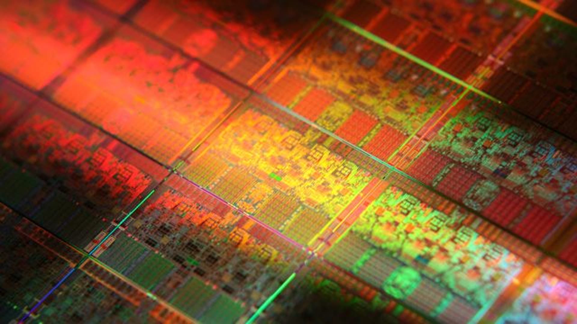
The excess material is polished off.![Metal Layers]() Multiple metal layers are created to connect the various transistors (they're just like wires). These connections are determined by the architecture and design teams that develop the functionality of the processor. While computer chips look extremely flat, they may actually have over 20 of these layers, forming complex circuitry. If you look at a magnified view of a chip, you will see an intricate network of circuit lines and transistors that look like a futuristic, multi-layered highway system.
Multiple metal layers are created to connect the various transistors (they're just like wires). These connections are determined by the architecture and design teams that develop the functionality of the processor. While computer chips look extremely flat, they may actually have over 20 of these layers, forming complex circuitry. If you look at a magnified view of a chip, you will see an intricate network of circuit lines and transistors that look like a futuristic, multi-layered highway system.![Wafer Sort Test]() This fraction of a ready wafer is put to a functionality test. In this stage test patterns are fed into every single chip and the response from the chip monitored and compared to "the right answer."
This fraction of a ready wafer is put to a functionality test. In this stage test patterns are fed into every single chip and the response from the chip monitored and compared to "the right answer."![Wafer Slicing]() The wafer is cut into individual pieces (called dies, they're a familiar rectangular shape even though they come from a round wafer) that are the heart of the processors that run our computers.
The wafer is cut into individual pieces (called dies, they're a familiar rectangular shape even though they come from a round wafer) that are the heart of the processors that run our computers.![Packaging]() Three elements are put together to form a completed processor. The green substrate builds the electrical and mechanical interface for the processor to interact with the rest of the PC. The silver heatspreader is a thermal interface that a cooling device will be placed on.
Three elements are put together to form a completed processor. The green substrate builds the electrical and mechanical interface for the processor to interact with the rest of the PC. The silver heatspreader is a thermal interface that a cooling device will be placed on.![Completed Processor]() A microprocessor is the most complex manufactured product on earth. In fact, it takes hundreds of steps — only the most important ones have been shown here — in the world's cleanest environment (a microprocessor fab, or fabrication plant) to make them.
A microprocessor is the most complex manufactured product on earth. In fact, it takes hundreds of steps — only the most important ones have been shown here — in the world's cleanest environment (a microprocessor fab, or fabrication plant) to make them.From Sand to Silicon: How a CPU Is Made
Ever wonder how Intel makes a CPU? Here's a glimpse at some of the amazingly sophisticated work going on daily inside those cutting-edge fabrication plants.


Move Forward
- From Sand to Silicon: How a CPU Is Made


